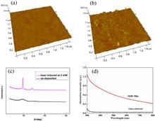
A Te-free binary phase change material SbBi is proposed as a new inorganic photoresist for heat-mode lithography. It shows good film-forming ability (surface roughness <1 nm), low threshold power for crystallization (2 mW), and high etching selectivity (15:1). Line-type, dot-type, and complex pattern structures with the smallest feature size of 275 nm are fabricated on SbBi thin films using a 405 nm diode laser direct writing system. In addition, the excellent grating structures with a period of 0.8 μm demonstrate that thermal interference does not affect the adjacent microstructures obviously. These results indicate that SbBi is a promising laser heat-mode resist material for micro/nanostructure fabrication.
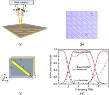
We propose and experimentally demonstrate a wideband linear polarization converter in a reflection mode operating from 2.4 to 4.2 THz with conversion efficiency of more than 80%. Our device can expand the applications to a higher frequency band. A numerical simulation is performed for this metamaterial converter, which shows a good agreement with experimental results. Importantly, a concise and intuitive calculating model is proposed for the Fabry–Pérot cavity. The theoretical results indicate that the underlying reason for the enhanced polarization conversion is the additional phase difference induced by the resonance of the meta-structure and multiple reflections within the Fabry–Pérot cavity.
A λ/4–λ/4 broadband antireflective (AR) coating is developed with a sol-gel dip-coating method. By adding SAR-5 organosilicon resin into a base-catalyzed silica sol top layer and treating at 300°C, a broadband AR coating used for blast shields with a high average transmission of 99.34% (450–950 nm) and good hydrophobicity (with a water-contact angle of 119°) was obtained. After being subjected to rubbing 50 times and being maintained at a relative humidity of around 95% for 50 days, the average transmission of the coating decreased by 0.29% and 0.04%, respectively. This indicates that the organically modified silica (ORMOSIL) broadband AR coating has good abrasion resistance and humidity stability.
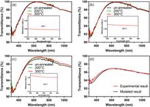
The effect of thermal annealing on the optical properties, microstructure, and laser-induced damage threshold (LIDT) of HfO2/Ta2O5/SiO2 HR films has been investigated. The transmission spectra shift to a short wavelength and the X-ray diffraction peaks of monoclinic structure HfO2 are enhanced after thermal annealing. The calculated results of the m( 111) diffraction peak show that the HfO2 grain size is increased, which is conducive to increasing the thermal conductivity. Thermal annealing also reduces the laser absorption of high-reflection films. The improvement of thermal conductivity and the decrease of laser absorption both contribute to the improvement of LIDT. The experimental results show that the highest LIDT of 22.4 J/cm2 is obtained at 300°C annealing temperature. With the further increase of annealing temperature, the damage changes from thermal stress damage to thermal explosion damage, resulting in the decrease of LIDT.
The cavity ring-down (CRD) technique is adopted for simultaneously measuring s- and p-polarization reflectivity of highly reflective coatings without employing any polarization optics. As the s- and p-polarized light trapped in the ring-down cavity decay independently, with a randomly polarized light source the ring-down signal recorded by a photodetector presents a double-exponential waveform consisting of ring-down signals of both s- and p-polarized light. The s- and p-polarization reflectivity values of a test mirror are therefore simultaneously determined by fitting the recorded ring-down signal with a double-exponential function. The determined s- and p-polarization reflectivity of 30° and 45° angle of incidence mirrors are in good agreement with the reflectivity values measured with the conventional CRD technique employing a polarizer for polarization control.
Specimens of PbTe single film are deposited on Ge substrates by vacuum thermal evaporation. During the temperature range of 80–300 K, the transmittance of a PbTe film within 2–15 μm is measured every 20 K by the PerkinElmer Fourier transform infrared spectroscopy cryogenic testing system. Then, the relationship between the refractive index and wavelength within 7–12 μm at different temperatures is received by the full spectrum inversion method fitting. It can be seen that the relationship conforms to the Cauchy formula, which can be fitted. Then, the relationship between the refractive index of the PbTe film and the temperature/wavelength can be expressed as n(λ,T)=5.82840 0.00304T+4.61458×10 6T2+8.00280/λ2+0.21544/λ4, which is obtained by the fitting method based on the Cauchy formula. Finally, the designed value obtained by the formula and the measured spectrum are compared to verify the accuracy of the formula.
An antireflection (AR) coating is fabricated by applying an optimal spin-coating method and a pH-modified SiO2 nanoparticle solution on a cover glass. Because the pH value of the solution will affect the aggregation and dispersion of the SiO2 particles, the transmittance of the AR-treated cover glass will be enhanced under optimal fabricated conditions. The experimental results show that an AR coating fabricated by an SiO2 nanoparticle solution of pH 11 enhances the transmittance approximately by 3% and 5% under normal and oblique incident conditions, respectively. Furthermore, the AR-treated cover glass exhibits hydrophobicity and shows a 65% enhancement at a contact angle to bare glass.
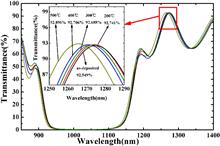
To simultaneously obtain high-resolution multi-wavelength (from visible to near infrared) tomographic images of the solar atmosphere, a high-performance multi-wavelength optical filter has to be used in solar imaging telescopes. In this Letter, the fabrication of the multi-wavelength filter for solar tomographic imaging is described in detail. For this filter, Ta2O5 and SiO2 are used as high- and low-index materials, respectively, and the multilayer structure is optimized by commercial Optilayer software at a 7.5° angle of incidence. Experimentally, this multi-wavelength optical filter is prepared by a plasma ion-assisted deposition technique with optimized deposition parameters. High transmittance at 393.3, 396.8, 430.5, 525, 532.4, 656.8, 705.8, 854.2, 1083, and 1565.3 nm, as well as high reflectance at 500 and 589 nm are achieved. Excellent environmental durability, demonstrated via temperature and humidity tests, is also established.
To improve the optical performance of an antireflection (AR) coating on a micro-spherical substrate, the ray angle of the incidence distribution and the thickness profile are taken into consideration during the optical coating design. For a convex spherical substrate with a radius of curvature of 10 mm and a clear aperture of 10 mm, three strategies are used for the optimization of the spectral performance of a broadband AR coating in the spectral region from 480 to 720 nm. By comparing the calculated residual reflectance and spectral uniformity, the developed method demonstrates its superiority in spectral performance optimization of an AR coating on a micro-spherical substrate.
The Pd/B4C multilayer is a promising candidate for high reflectance mirrors operating in the 8–12 nm extreme ultraviolet wavelength region. To extend the working bandwidth beyond the L-edge of silcon, we theoretically design broadband Pd/B4C multilayers. We discuss the influence of the desired reflectance of the plateau, number of bilayers, and the real structural parameters, including the interface widths, layer density, and thickness deviation, on the reflectivity profile. Assuming the interface width to be 0.6 nm, we design aperiodic multilayers for broad wavebands of 9.0–10.0, 8.5–10.5, and 8.0–11.0 nm, with average reflectivities of 3.1%, 5.0%, and 9.5%, respectively.
Molybdenum (Mo) thin films, most commonly used as electrical back contacts in Cu(In,Ga)Se2 (CIGS) solar cells, are deposited by rf and dc magnetron sputtering in identical systems to study the discrepancy and growth mechanisms of the two sputtering techniques. The results reveal that though different techniques generally deposit films with different characteristic properties, Mo films with similar structural and physical properties can be obtained at respective suitable deposition conditions. Highly adhesive and conductive Mo films on soda lime glass are further optimized, and the as-fabricated solar cells reach efficiencies as high as 9.4% and 9.1% without an antireflective layer.
The mechanism of ferromagnetic ordering in ZrOx film is investigated by both experimental observation and theoretical calculation. Magnetic measurements reveal that the magnetic properties can be adjusted from diamagnetism to ferromagnetism by varying the oxygen stoichiometry. We find that oxygen-rich defects can be responsible for the observed magnetic properties by taking the measurements of x-ray photoelectron spectroscopy and room temperature photoluminescence spectra. Density functional theory calculations further confirm that the ferromagnetic order is mainly driven by the exchange interaction between the oxygen antisites and the neighboring anion atoms.
A lateral photovoltaic effect (LPE) is discovered in an LaTiO3+δ film epitaxially grown on a (100) SrTiO3 substrate. Under the illumination of a continuous 808 nm laser beam that is focused on the LaTiO3+δ film through the SrTiO3 substrate, the open-circuit photovoltage depends linearly on the illuminated position. The sensitivity of the LPE can be modified by the bias current. The LaTiO3+δ film shows a stable photoelectric property under the high pressure, up to 9 MPa. These results indicate that the LaTiO3+δ films can give rise to a potentially photoelectronic device for near-infrared position-sensitive detection in high-pressure environments.
The defect evolution is investigated for high-reflective coatings under multiple irradiations with an improved statistical model. The fatigue effect is observed with an increase in the shot numbers, but the fatigue process will not endure and it tends to be saturated when the number of shots reaches a certain level. With the addition of a bilayer unit, the defect density distribution of the high-reflective coatings is obtained. Two defect types are identified, and the differentiation of the high-damage precursors can well explain the decrease of the laser-induced damage threshold, as well as the saturation effect.
We investigate the 120 keV hydrogen ion-implanted LiTaO3 samples. To observe the implantation-induced crystal structure and composition changes we use Raman scattering, infrared spectroscopy, and cross-section transmission electron microscopy. In addition, elastic recoil detection analysis is used to detect the hydrogen concentration. Experimental results show that hydrogen ions mainly participate in the formation of platelets and micro-cracks, and diffuse out during the thermal process. Only a small portion of hydrogen is attached to the Li site and Li vacancy to form O-H. The content decrease of Li after hydrogen implantation was discussed.
Light-induced transverse thermoelectric effect is investigated in incline-oriented Bi2Sr2Co2Oy thin films covered with a graphite light absorption layer. Upon the illumination of a 980 nm cw laser, an enhanced voltage signal is detected and the improvement degree is found to be dependent on the thickness of the graphite layer. A two-dimensional (2D) heat transport model using the finite-difference method provides a reasonable explanation to the experimental data. Present results give some valuable instructions for the design of light absorption layers in this type of detector.
A Closed Cavity measuring platform is built on the basis of a 1000 W-class direct current (DC)-discharge drived continuous-wave (CW) HF/DF chemical laser. On this platform, the absorption coefficients of optical thin films coated on the surfaces of monocrystalline silicon substrates, at the wavelength of 3.6–4.1 μm, is measured, when the power density on the surfaces of optical thin films reaches about 3.16 kW/cm2. The measuring principle and structure of the Closed Cavity is introduced. The temperature curves and balanced temperature rises of the film-substrate systems under test measured through the experiment is presented in this Letter. The experiments show high reliability, good repeatability and strong practicality. The Closed Cavity measuring platform is applicable for not only absorption measurement but other performance measurement of optical thin films under high power density.
We prepare SiO2 coatings on different substrates by either electron-beam evaporation or dual ion-beam sputtering. The relative transmittances of the SiO2 coatings are measured during the heating process. The SiO2 coating microstructures are studied. Results indicate that the intensity and peak position of moisture absorption are closely related to the microstructures of the coatings. The formation of microstructures depends not only on the preparation process of the coatings but also on the substrate characteristics.
In our investigation, lead germanium telluride, which is a pseudo-binary alloy of IV-VI narrow-gap semiconductor compounds of PbTe and GeTe, can be used in the fabrication of mid-wavelength infrared narrow bandpass filters as a high-index coating material, due to its high refractive index, lower absorption, and tunability of fundamental absorption edges. It is demonstrated that a half-width of 160 nm and a better rejection ratio can be obtained for a simple 8-layer double cavity filter with a central wavelength at 4 μm, compared with a half-width of 390 nm for those conveniently fabricated using Ge as high-index material.
A number of zinc oxide (ZnO) films are deposited on silicon substrates using the magnetron sputtering method. After undergoing thermal treatment under different conditions, those films exhibit hexagonal wurtzite structures and different photoluminescent characteristics. Besides the notable ultraviolet emission, which is related to the free exciton effect, a distinct blue fluorescence around 475 nm is found in some special samples. The blue photoluminescence emission of the ZnO film is believed to be caused by oxygen vacancies.
The influence of technique parameters on the temperature coefficient of resistance (TCR) of reduced graphene oxide (RGO) films is studied. These technique parameters include the ultrasonic time, solution concentration, and heat treatment temperature. Results show that, the best technique parameters are ultrasonic time of 14 h, solution of 0.12 ml, and annealing temperature of 800 oC, and on this point, TCR value of RGO is from -0.67% to -1.36% at the different film thicknesses.
A Terahertz sensing method based on the resonant transmission characteristics through metallic aperture arrays is proposed. Here we present metallic aperture arrays of rectangular and H-shaped holes which induce localized resonance. High characterization sensitivity to surface condition is demonstrated. When applied with the liquid of 3-pentanone, arrays of rectangular and H-shaped holes have sensitivity of 158 and 172 GHz/RIU (refractive index unit), respectively. So the metal meshes based localized resonance can also be used as a sensor chip in terahertz region.
SiC coating for surface modification grows on reaction boned SiC (RB-SiC) substrate cannot have high quality because the material of RB-SiC has two phases. We apply a new method to improve the effect of surface modification. First the surface of RB-SiC is carbonized, and then a diamond like carbon (DLC) coating is prepared on it before the growth of SiC coating. Research and tests show that the SiC coating can grow denser and uniform because of the buffer function of the DLC coating, thus the effect of surface modification is improved. The roughness reduces from 1.397 to 0.478 nm (rms) after the surface modification using DLC buffer layer.
The roles of laser-induced defects and native defects in multilayer mirrors under multi-shot irradiation condition are investigated. The HfO2/SiO2 dielectric mirrors are deposited by electron beam evaporation (EBE). Laser damage testing is carried out on both the 1-on-1 and S-on-1 regimes using 355-nm pulsed laser at a duration of 8 ns. It is found that the single-shot laser-induced damage threshold (LIDT) is much higher than the multi-shot LIDT. In the multi-shot mode, the main factor influencing LIDT is the accumulation of irreversible laser-induced defects and native defects. The surface morphologies of the samples are observed by optical microscopy. Moreover, the number of laser-induced defects affects the damage probability of the samples. A correlative model based on critical conduction band (CB) electron density (ED) is presented to simulate the multi-shot damage behavior.
A-plane GaN films are deposited on (302) \gamma-LiAlO2 substrates by metalorganic chemical vapor deposition (MOCVD). The X-ray diffraction (XRD) results indicate that the in-plane orientation relationship between GaN and LAO substrates is [010]LAO//[0001]GaN and [203]LAO//[1100]GaN with 0.03% and 2.85% lattice mismatch, respectively. Raman scattering results indicate that the strain in the films decreases along with the increase in the thickness of the films. In addition to the band edge emission at 3.42 eV, defects-related luminescence at 3.35 eV is observed in the photoluminescence (PL) spectra. The cathodoluminescence (CL) spectra indicate that the 3.35-eV emission is related to the V pits.
Single-pulse and multi-pulse damage behaviors of "standard" (with \lambda/4 stack structure) and "modified" (with reduced standing-wave field) HfO2/SiO2 mirror coatings are investigated using a commercial 50-fs, 800-nm Ti:sapphire laser system. Precise morphologies of damaged sites display strikingly different features when the samples are subjected to various number of incident pulses, which are explained reasonably by the standing-wave field distribution within the coatings. Meanwhile, the single-pulse laser-induced damage threshold of the "standard" mirror is improved by about 14% while suppressing the normalized electric field intensity at the outmost interface of the HfO2 and SiO2 layers by 37%. To discuss the damage mechanism, a theoretical model based on photoionization, avalanche ionization, and decays of electrons is adopted to simulate the evolution curves of the conduction-band electron density during pulse duration.
We report a new structure for broadband antireflection coating by dip-coating technique, which has minimal cost and is compatible with large-scale manufacturing. The coatings are prepared by depositing SiO2 sol-gel film on a glass substrate, subsequently depositing SiO2 single-layer particle coating through electrostatic attraction, and depositing a final very thin SiO2 sol-gel film to improve the mechanical strength of the whole coating structure. The refractive index of the structure changes gradually from the top to the substrate. The transmittance of a glass substrate has been experimentally found to be improved in the spectral range of 400-1,400 nm and in the incidence angle range from 0o to at least 45o. The mechanical strength is immensely improved because of the additional thin SiO2 sol-gel layer. The surface texture can be applied to the substrates of different materials and shapes as an add-on coating.
We prepare Six(ZrO2)100?x composite films using the co-sputtering method. The chemical structures of the films which are prepared under different conditions are analyzed with X-ray photoemission spectroscopy. Thermal treatment influences on optical property and resistance switching characteristics of these composite films are investigated by spectroscopic ellipsometry and semiconductor parameter analyzer, respectively. With the proper Si-doped Six(ZrO2)100?x interlayer, the Al/ Six(ZrO2)100?x/Al device cell samples present very reliable and reproducible switching behaviors. It provides a feasible solution for easy multilevel storage and better fault tolerance in nonvolatile memory application.
Using e-beam evaporation, the ellipsometric parameters of thick transparent films are studied with the modified analysis method for the SiO2 film samples deposited onto the Si substrate. The ellipsometric parameters are measured at the incidence angles changing from 50? to 70? and in the 3–4.5 eV photon energy range. The error in the conventional method can be significantly reduced by the modified ellipsometric method considering the spatial effect to show good agreement between the theoretical and experimental results. The new method presented in this letter can be applied to other optical measurement of the periodic or non-periodic film structures.
Ultra-narrow linewidth, nonpolarizing guide-mode resonance (GMR) filters with single and double common resonance wavelengths are designed. The guide-mode resonance filters consist of a single grating layer with asymmetric profiles. By choosing appropriate parameters, same resonance wavelengths for both transverse electric (TE) and transverse magnetic (TM) polarizations can be achieved. Results show that high reflection (more than 99.9%) is obtained at every resonance wavelength, and the full-width at half-maximums (FWHMs) of TE- and TM-polarized light are only 0.008 and 0.215 nm, respectively.


